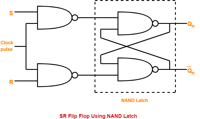
Gated SR Flip-Flop (NAND) – Interactive
Toggle S, R, and CLK inputs and observe the flip-flop state. **CLK=1** enables operation.
S:
R:
CLK:
Outputs:
Q0
Q̅1
Circuit Diagram
[Image of SR Latch using NAND gates circuit diagram]
Timing Diagram (S-R Combinations at CLK=1)
Current: S=0, R=0, CLK=0 → Hold State (CLK Disabled) (Q=0, Q̅=1)
Comments
Post a Comment